
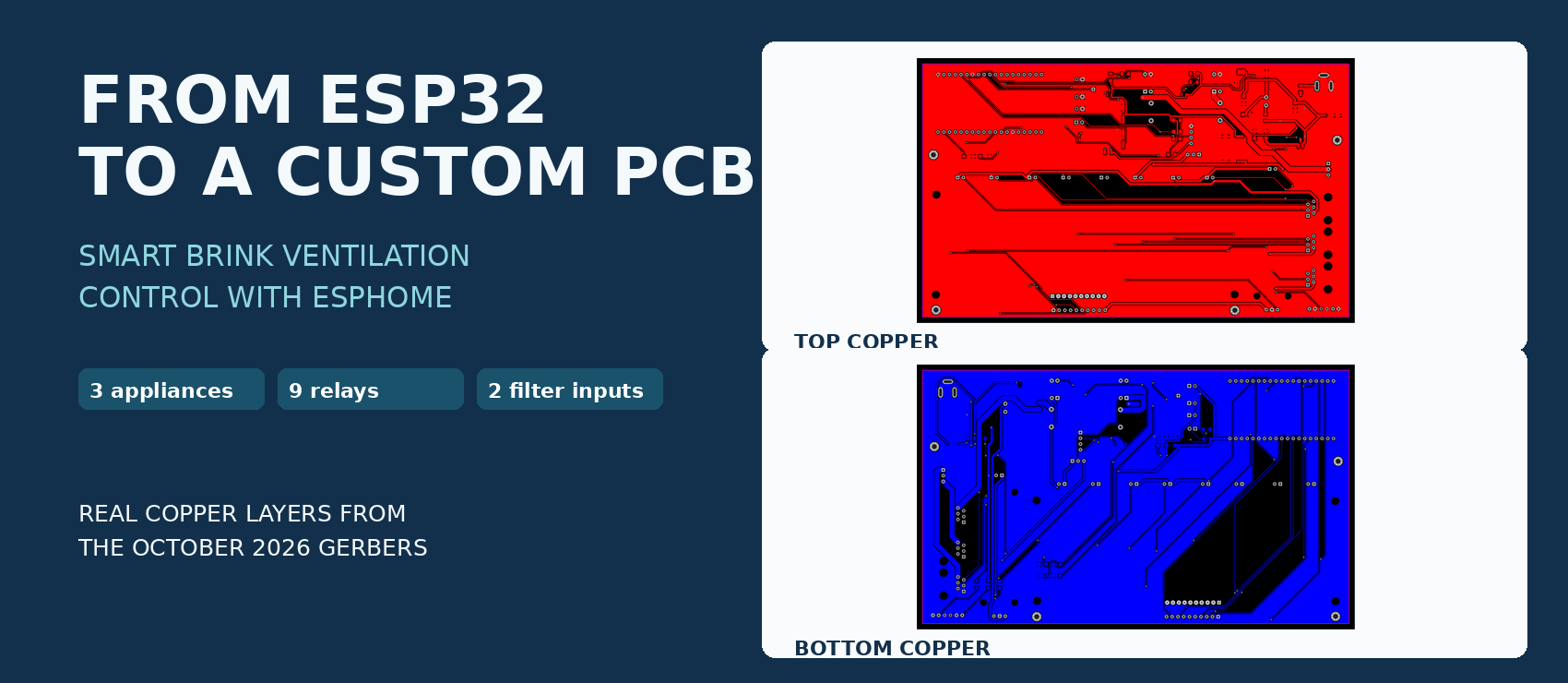
Nine relays, three separate Brink connectors, optically isolated filter detection and an ESP32: a working DIY controller has grown into a custom circuit board. This article explains what the controller does, how its electronics are designed and which choices matter when controlling ventilation systems with Home Assistant and ESPHome.
Project status — October 2026. This article describes the current EasyEDA schematic and PCB design files. The existing ESPHome relay setup was the starting point; this does not automatically validate the new physical PCB electrically, thermally, mechanically or over time. Elan filter measurements, relay-module variants, footprint mappings and final hardware tests remain open. The copper-layer images are a Gerber design visualisation, not photographs of a fully tested controller.
1. Why design your own PCB?
An ESP32 and relay module make an excellent way to test an automation idea. Connect GPIOs, configure ESPHome and let Home Assistant command the desired functions. In the original setup, one ESP controlled the fan settings of a Brink Renovent and two separate zones of a Brink Elan E.
A prototype makes it easy to exchange parts, try GPIOs and change wiring without redesigning a board. As functions are added, however, the number of loose wires, supply connections, terminals and small boards grows. Documentation and troubleshooting become harder. A contact that seemed obvious while building may be difficult to identify months later.
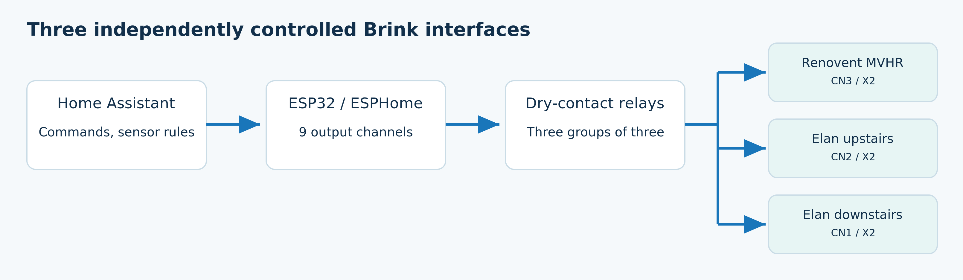
The custom PCB does not replace Brink’s operation. It brings existing functions together: connectors for three units, a relay interface, two filter-detection channels, power, programming and status functions. It still uses complete external relay modules. “Custom PCB” does not mean that every relay is constructed from discrete parts on its copper traces.
Designing a board also forces you to consider current paths, signals versus supply rails, transistor pinouts, decoupling capacitors and which electrical references may or may not be joined. Those choices determine whether an understandable schematic can become a usable physical board.
2. What exactly does the board control?
| PCB connector | Unit/function | Available control |
|---|---|---|
| CN3 | Brink Renovent Excellent 300/400 HRV | Three closing contacts; a fourth logical position with all contacts open |
| CN2 | Upper Brink Elan E zone | The same relay principle for the upper zone |
| CN1 | Lower Brink Elan E zone | The same relay principle for the lower zone |
The Renovent is the HRV unit: it extracts indoor air and supplies outdoor air with heat recovery. The Elan E is an air heater with separate ventilation zones. Zone control can influence air movement, but the PCB does not replace Elan’s internal safety, heating control or thermostat logic.
Two filter-detection channels are added: one for the Renovent and one switched by jumpers to the chosen Elan zone, not three simultaneous filter measurements. The board also has LEDs, an indicative 5V measurement, buzzer output, programming connectors and a reserved PWM output.
“Positions 1 through 4” denote logical ESPHome contact combinations. Brink setting names, configured airflow and priority between internal controls vary by model and configuration. Do not equate those terms without testing the unit.
3. How the complete system works
Home Assistant provides controls, dashboards and automations. ESPHome translates commands into GPIO outputs and reads digital inputs. The PCB is the physical interface to the Brink connectors. Neither Home Assistant nor the ESP32 directly drives motors through Brink’s internal board; Brink remains responsible for its own fan control and safety provisions.
This differs from driving a fan directly with PWM. The relays simulate an existing wired selector switch. It is clearer than intervening in internal power circuitry, but still requires correct connection to the intended low-voltage port.
4. RJ12 is the key interface
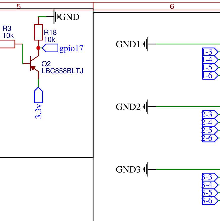
On the Renovent Excellent described here and both Elan E zones, X2 provides a modular RJ12 connector for selector control. Brink marks it as low voltage only, not 230 V. In the custom schematic, nets are named by device and contact, for example 1-3 for HRV pin 3. The return is deliberately separate for each device: GND1 for HRV, GND2 for upper Elan and GND3 for lower Elan. None is interchangeable with ESP-GND because of its name.
| RJ12 contact | Function in this design | Limitation |
|---|---|---|
| Pin 1 | Not connected on the custom PCB | May supply internal auxiliary power on a supported Renovent variant; do not connect to external 5 V. |
| Pin 2 | Common/return for the specific Brink channel | To COM on only that channel’s three relays. |
| Pin 3 | First selector input | Dry NO contact to pin 2. |
| Pin 4 | Second selector input | Dry NO contact to pin 2. |
| Pin 5 | Third selector input | Dry NO contact to pin 2. |
| Pin 6 | Filter indication input | Measure voltage/polarity first; through optocoupler, never directly to GPIO. |
This is the custom PCB pinout, not a universal RJ12 standard or guarantee for every Brink model and filter voltage. Check the exact unit, connector viewpoint and cable. Six visible contacts or familiar wire colours do not establish a correct cable. With power off, use a continuity tester to determine which physical RJ12 position leads to each conductor or PCB pad. Record the latch orientation to avoid a mirrored pin view.
5. Why nine relays for four logical positions?
The ESP32 drives a relay module through GPIO; COM/NO contacts remain electrically separate from that GPIO. Energising joins COM and NO; releasing opens the contact. The PCB thus imitates a mechanical selector without injecting its own logic voltage into a Brink control line.
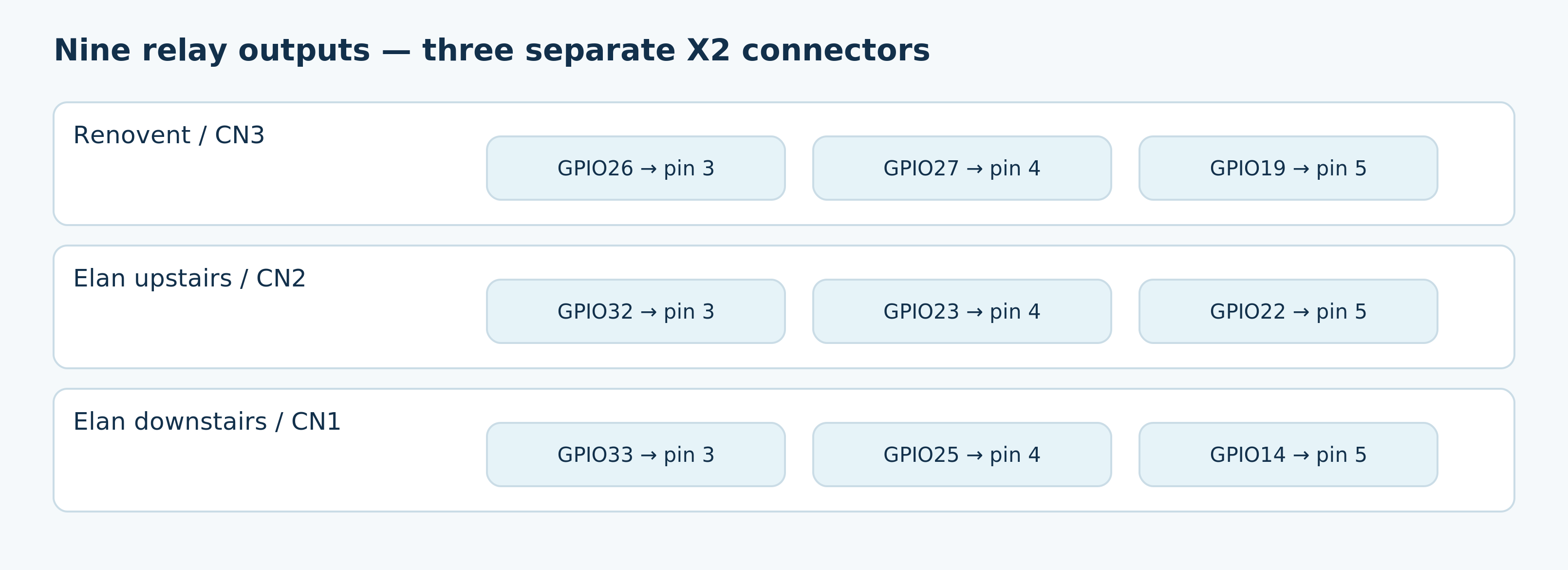
Each Brink connector offers three selector contacts. Closing at most one at a time gives four combinations: all open or one of three closed. The original ESPHome code uses interlock within each group. This prevents deliberate simultaneous activation during normal firmware operation, but is not a hardware lock for resets, wrong active-low logic or welded contacts.
| Unit / PCB | ESPHome position 1 | Position 2: pins 2–3 | Position 3: pins 2–4 | Position 4: pins 2–5 |
|---|---|---|---|---|
| Renovent / CN3 | All open → Brink setting 1 here | GPIO26 → Brink setting 0 | GPIO27 → Brink setting 2 | GPIO19 → Brink setting 3 |
| Upper Elan / CN2 | All open; unit-dependent effect | GPIO32 | GPIO23 | GPIO22 |
| Lower Elan / CN1 | All open; unit-dependent effect | GPIO33 | GPIO25 | GPIO14 |
The Renovent mapping follows the project-specific practical Excellent 300/400 pinout. Elan zones follow their own programmes; do not label their positions 0/1/2/3 or assign fixed airflow without separate verification. All relays off is the contact-free base position, not necessarily the lowest Brink operating setting. Setting 0 does not itself guarantee required minimum ventilation.
An eight-channel module plus a separate one-channel module provides nine outputs. Headers and short external wires connect them to the board. J1/J2, H1–H10 and module IN1–IN8 must be tested on the built assembly. Power for the eight-channel module passes through U6, Schottky diode D1 (1N5819) and C1/C2. D1 causes voltage drop: test that the chosen 5V modules reliably energise and release under load with 3.3V GPIO drive. The 1000ah marking at U6 is not a valid electrical unit; confirm the final current value and part in the BOM.
On power loss, normal de-energised NO contacts open. Brink then assumes the state associated with those open contacts. This is an intended recovery behaviour to verify with installed modules and the actual Brink configuration. Software interlocks do not prevent wrongly wired NC, reversed trigger logic, contact welding or boot pulses.
6. The 5V supply: simple but deliberate
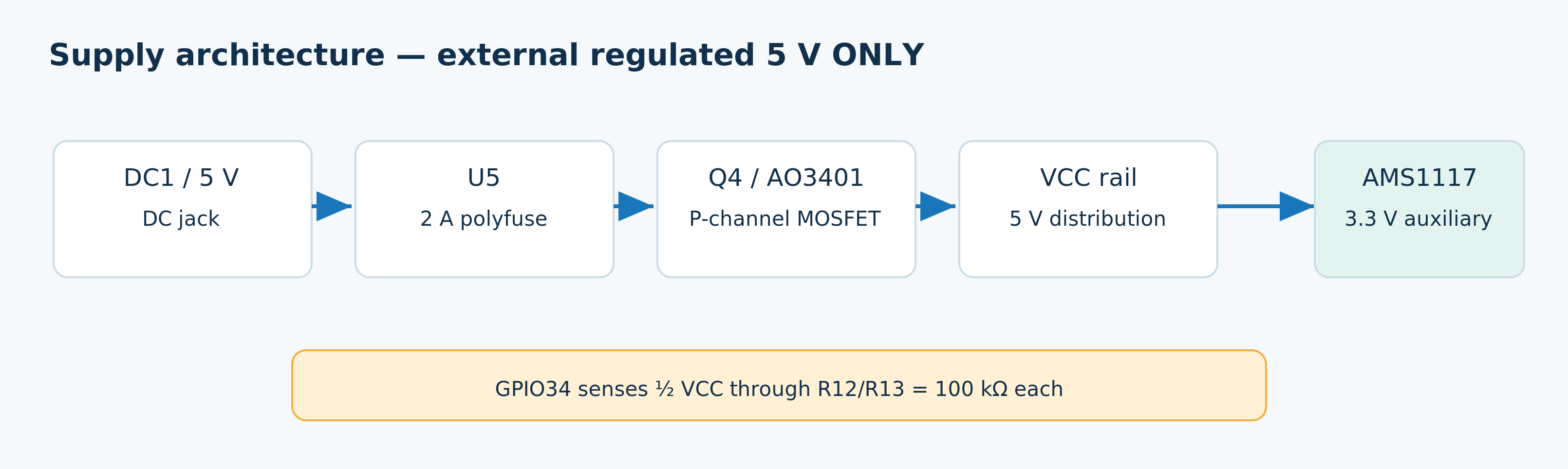
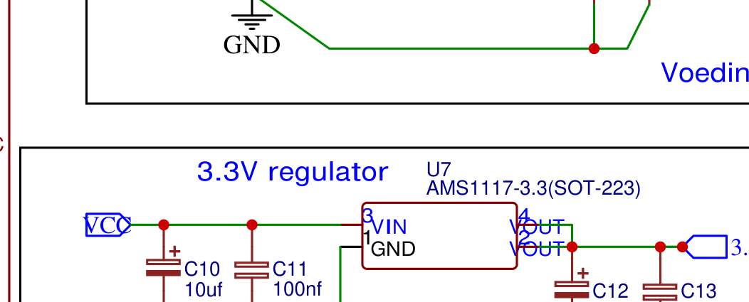
The PCB uses only an external regulated 5V adapter. Power enters through DC jack DC1, then passes 2A polyfuse U5 and P-channel MOSFET Q4 (AO3401) designed for reverse-polarity protection. A MOSFET may reduce voltage drop compared with a series diode, provided its real pin-to-footprint mapping is correct. R14 of 10 kΩ pulls Q4’s gate to ground.
VCC runs directly to the ESP32 DevKit’s 5V input and relay supply. There is no 12V-to-5V converter; a 12V or 24V adapter can damage parts. A polyfuse does not protect against a high but current-limited supply voltage. C3 (100 nF) filters fast noise and C4 (470 µF) buffers brief load changes. The positive side of a polarised electrolytic capacitor must face the positive rail. After Q4, VCC should remain close to 5 V on a correctly connected board, with possibly a small drop under load.
Schematic symbols may match while a chosen footprint assigns Q4’s physical source and drain differently. Check both datasheet and EasyEDA footprint, not just the symbol. Verify DC jack pins before applying power.
7. Separate 3.3V regulator and power monitoring
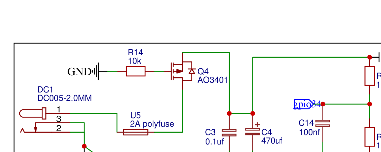
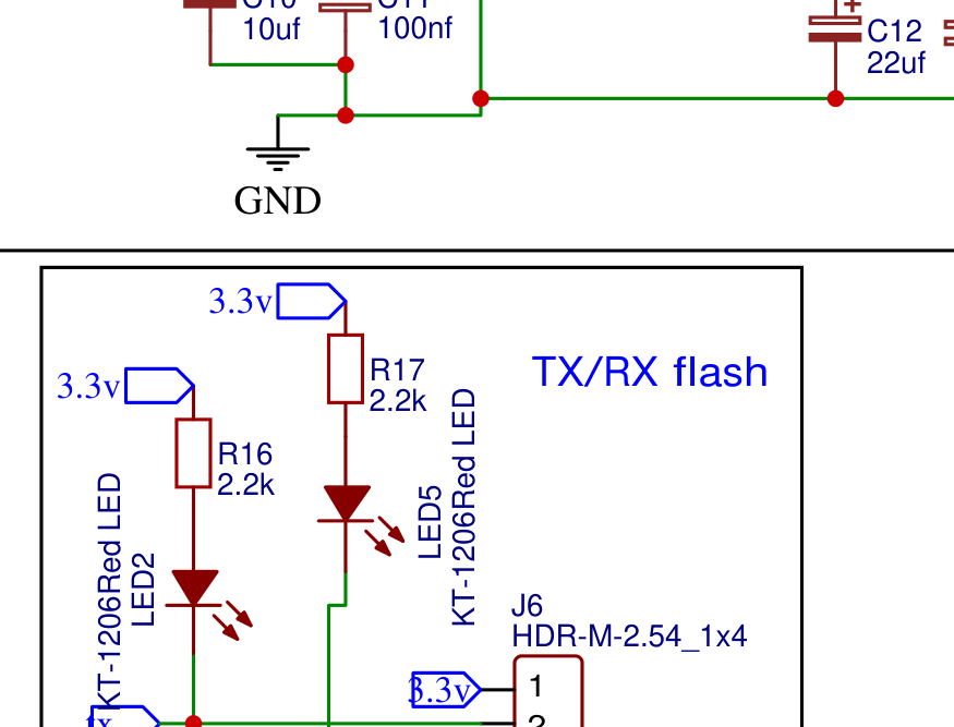
AMS1117-3.3 (U7) supplies a separate 3.3V rail for auxiliary circuitry. The DevKit receives 5 V and has its own regulator. Do not casually connect two 3.3V regulator outputs in parallel.
The drawn circuit uses C10 10 µF, C11 100 nF, C12 22 µF and C13 100 nF. The actual C12 type and ESR must suit the specific AMS1117 variant; loaded stability remains to be measured. A linear regulator turns voltage difference into heat: at 100 mA and a 1.7 V drop, approximately 0.17 W. Dissipation increases proportionally with added load. It can serve light auxiliary circuits but is not automatically suitable for heavy 3.3V loads.
R12/R13, each 100 kΩ, halve the 5V rail. At VCC = 5.00 V, ideal GPIO34 input voltage is 2.50 V. C14 100 nF reduces noise. Calibrated ESPHome ADC readings can reveal a sagging supply, but cannot announce total power loss when the ESP32 itself is no longer running.
8. Filter sensing with PC817 and BC858
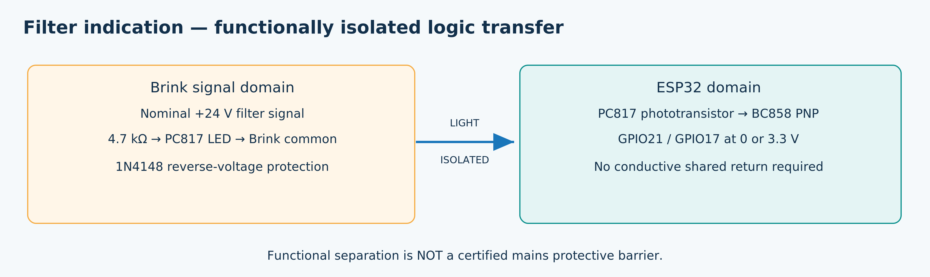
An ESP32 GPIO expects 3.3V logic. A filter line that might supply about 24 V on an alert must never connect directly to it. A PC817 has an LED on the Brink side and a phototransistor on the ESP side; optical transfer keeps the circuits functionally separate. This is not a certified mains safety barrier.
In the design, the filter line runs through 4.7 kΩ R1/R7 to the optocoupler LED; return goes to the common of that same Brink channel. D4/D5 (1N4148) are antiparallel to protect against reverse LED voltage. Assuming +24.0 V and 1.2 V LED forward voltage gives I = (24.0 − 1.2) / 4,700 ≈ 4.85 mA and about 0.11 W resistor dissipation. This is a theoretical check, not proof that either Elan filter line supplies +24 V. Measure the actual voltage, polarity and alert behaviour.
On the ESP side, collector pull-up, BC858 PNP stage and supporting resistors create intended active-HIGH logic: no alert = GPIO LOW, alert = around 3.3 V HIGH. OP1 routes the HRV alert to GPIO21; OP2 routes the chosen Elan zone to GPIO17. Because the transistor stage already inverts, ESPHome does not need another inverted: true. Filter indication processes an offered electrical signal; it does not measure filter pressure drop, dirt or air quality. Its meaning depends on Brink’s controller and maintenance settings and needs confirmation on the actual unit.
9. Why two Elan jumpers?
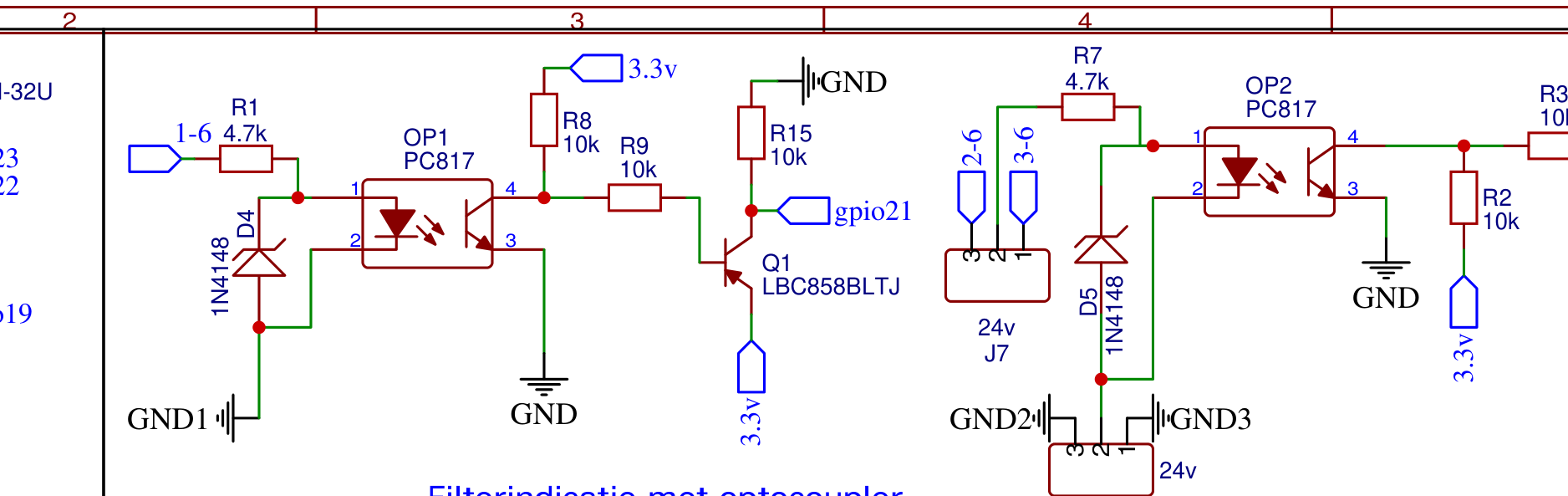
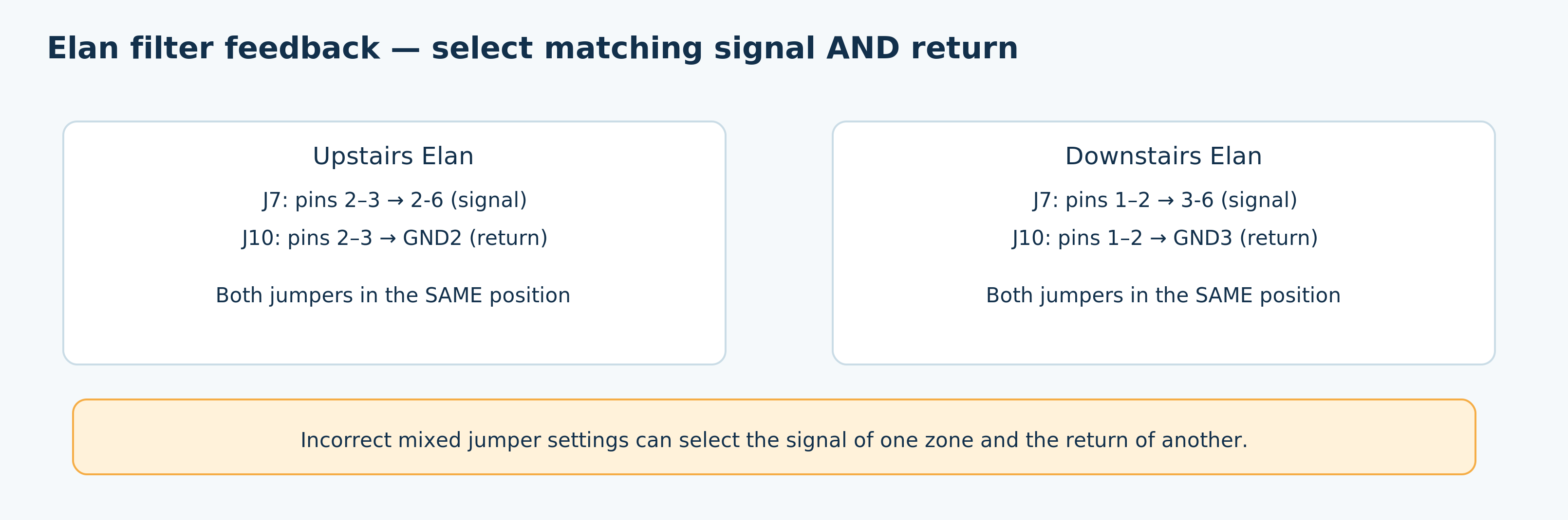
The two Elan E zones have separate X2 connectors. One Elan filter-detection channel must take both signal and return from the same zone. J7 chooses the pin-6 filter signal and J10 chooses its pin-2 common. Switching only the signal could measure it against the wrong zone’s common.
| Selected zone | J7, pin-6 signal | J10, pin-2 common |
|---|---|---|
| Upper Elan | Net 2-6, jumper 2–3 | GND2, jumper 2–3 |
| Lower Elan | Net 3-6, jumper 1–2 | GND3, jumper 1–2 |
Check physical header orientation and silkscreen labels. Always set both jumpers to the same zone; do not connect GND2/GND3 because their names resemble each other. The jumpers affect only the measured filter line, not normal relay-based ventilation control. A linked two-pole selector might reduce user error in a future revision.
10. Other PCB functions
Besides its relays and power circuits, the controller has service and diagnostic functions:
- Three status LEDs. A green power LED connects to VCC through a resistor; a red fault LED uses GPIO13 and a blue filter LED uses GPIO16. Software decides when the GPIO-driven LEDs light. An LED does not prove that an external fan is running; it represents a software selection or offered electrical input.
- UART and TX/RX indication. J6 exposes 3.3V reference, TX, RX and GND. Two SMD LEDs with 2.2kΩ resistors sit between 3.3 V and the UART lines. UART idles HIGH, so they are normally off and may light during LOW bits. Check the RX LED’s colour/part against the final BOM. Do not casually connect J6’s 3.3 V to a second active supply or use a 5V UART adapter directly.
- Flash and reset. Two push buttons pull GPIO0 and EN respectively to GND for serial firmware programming and ESP32 reset.
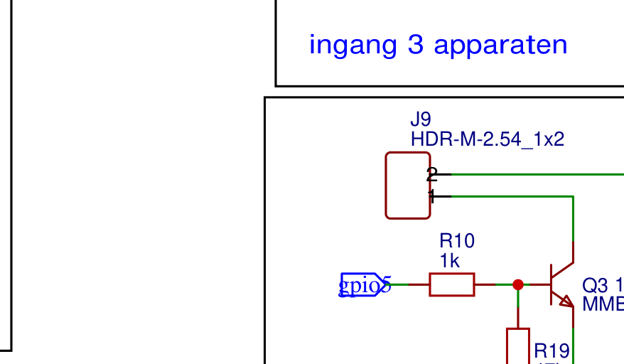
- Filter buzzer. GPIO5 drives the base of MMBT2222A Q3 through 1 kΩ R10. R19 of 47 kΩ holds the base low when GPIO is high-impedance. A separate 5V branch through R11 and C9 supplies the buzzer. This arrangement is intended for a suitable active buzzer; an electromagnetic type may need a flyback diode. GPIO5 is an ESP32 strapping pin, so check cold boot.
- Reserved PWM. GPIO18 reaches J8 for a possible future function. A normal four-wire fan usually needs a suitable output stage and shared signal reference; J8 alone is not a complete driver.
- External power and test points. Headers and test points make 5 V, 3.3 V and serial signals easier to measure, but need clear labels and protection against backfeeding from programming/test equipment.
11. The role of ESPHome and Home Assistant
The existing ESPHome configuration declares nine GPIO relays, interlocked in groups of three. Home Assistant can choose a position for the HRV, upper Elan and lower Elan independently. At the contact-free base position, a template action turns off all three contacts in that group. For this Renovent installation that means Brink setting 1, not “lowest possible setting”.
A simplified example of one relay in the current mapping:
switch:
  - platform: gpio
    name: "WTW positie 2"
    id: wtw_pos2
    pin: GPIO26
    restore_mode: ALWAYS_OFF
    # Interlock pas toe in de volledige groep met positie 3 en 4.
For filter inputs designed to go HIGH on an alert:
binary_sensor:
  - platform: gpio
    name: "WTW filtermelding"
    pin:
      number: GPIO21
      mode: INPUT
    device_class: problem
    filters:
      - delayed_on: 200ms
  - platform: gpio
    name: "Elan filtermelding geselecteerde zone"
    pin:
      number: GPIO17
      mode: INPUT
    device_class: problem
    filters:
      - delayed_on: 200ms
These fragments are illustrative, not a complete working configuration. The original YAML mainly had relays and device sensors. Production use requires testing restore modes, initial GPIO states, buzzer, LEDs, filter signals, connection loss and manual control on real hardware.
Home Assistant could request a higher setting for showers, cooking or CO₂, but those automations run on top of the PCB. Without separate CO₂ or relative-humidity sensors, the board cannot measure those values. An optimistic select shows a requested command, not proven relay closure or airflow.
12. Safety: where is the boundary?
The PCB connects to equipment containing internal 230V mains power. Keep Brink low voltage, ESP electronics and mains sharply separate:
- X2 low voltage only. RJ12 is not a 230V connector. A mechanically matching plug does not establish electrical compatibility. Mains on the PCB or RJ12 can cause fire, injury and damage. Do not inject external 5 V or 24 V into Brink selector contacts either.
- Separate the references. GND1, GND2 and GND3 are the three Brink commons; GND is ESP ground. Do not join them on the basis of their names. PC817 gives functional isolation for filter information, not proven protective insulation or product certification.
- Voltage-free really means voltage-free. COM/NO joins only two intended Brink pins. NC stays unused. Measure the physical contact state on loss of power; do not assume every module is active-high.
- A polyfuse does not solve everything. It limits fault current but not every wrong supply voltage or brief transient. Use regulated 5 V, a suitable connector/cable and prevent unwanted backfeed between external 5 V and DevKit USB.
- Software is only one layer.
interlockhelps with normal commands, not wrong wiring, welded relays or boot phases. Restart, Wi-Fi/Home Assistant failure and power loss must be predictable on the actual assembly. - Test in stages. Start with power-off continuity, shorts and connector orientation; then current-limited 5V bench power; connect Brink only after workbench tests. Power down Brink according to its manufacturer procedure before connection work.
This is a learning and development project. Neither the schematic, PCB nor article guarantees safe use in every installation. The selected setting must provide enough real airflow; prolonged under-ventilation is unacceptable. The liability statement below does not replace risk assessment or applicable installation and product-safety requirements.
13. From electrical schematic to physical PCB in EasyEDA
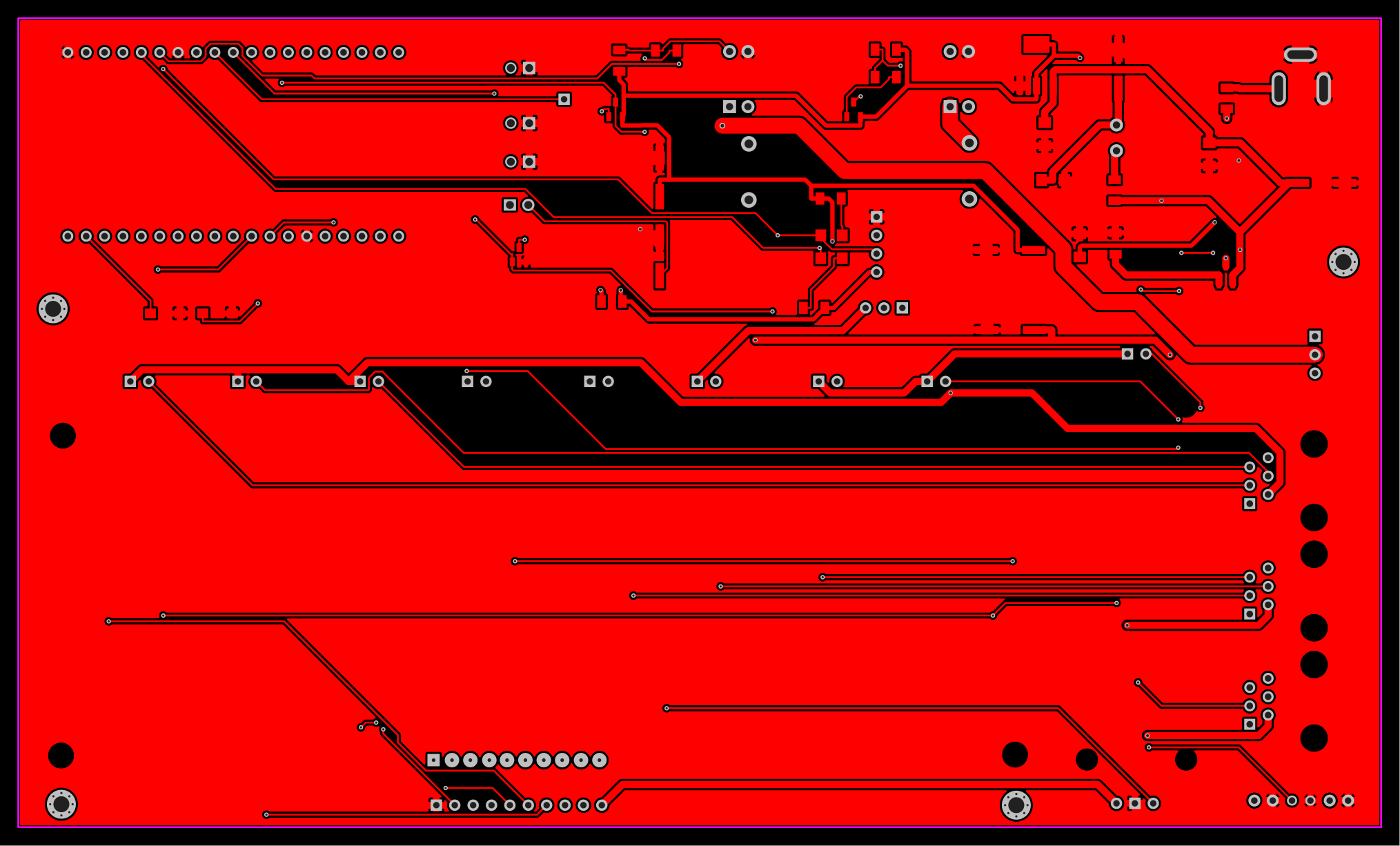
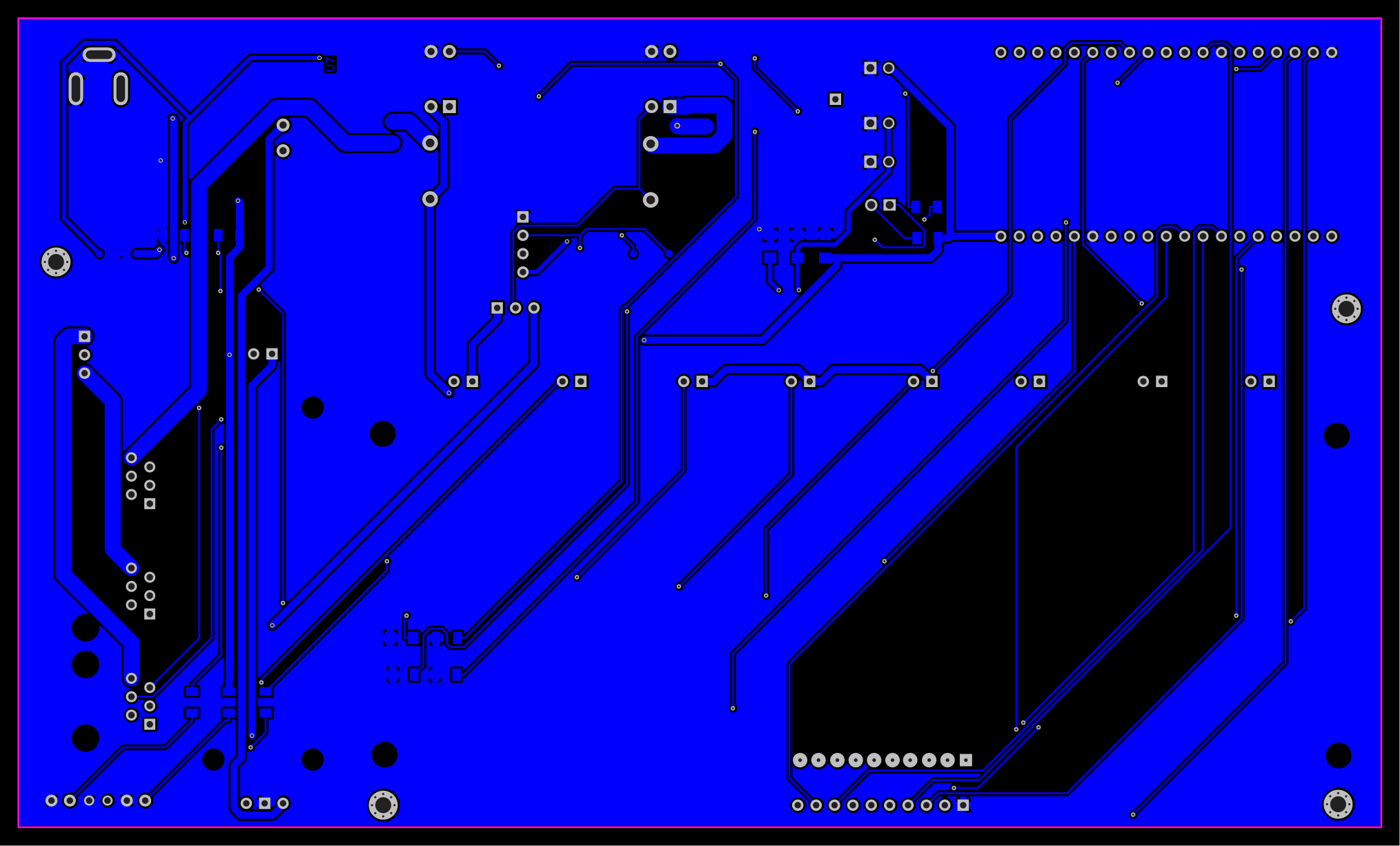
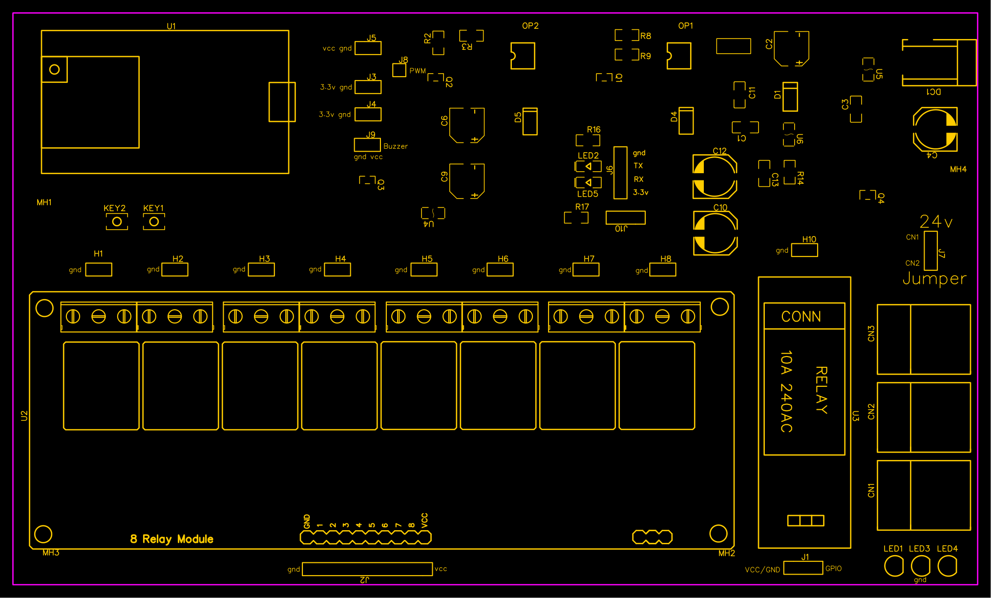
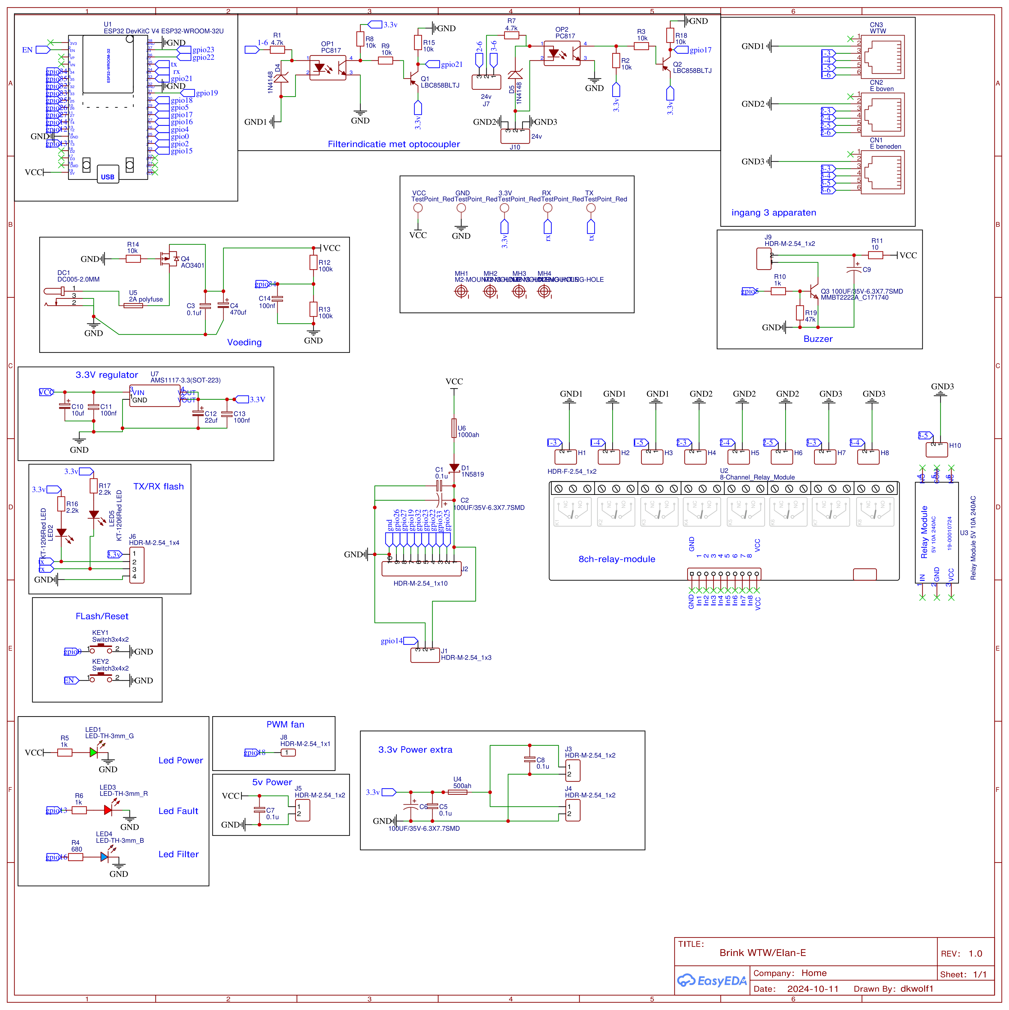
A schematic states which points must be connected electrically; a PCB layout specifies how copper implements those connections. A correct schematic may still produce a board with wrong footprints, insufficient clearance or missing connections.
In this design, DevKit, relay modules, RJ12 sockets and power components make a relatively large board. The Gerber export shows two copper layers, solder mask, silkscreen, vias, mounting holes and a closed board outline. An early visual fabrication review found copper edges relatively close to the board edge in places and some fine silkscreen details. These are manufacturing issues, not conclusions from circuit theory alone.
A useful sequence is to complete the schematic, map exact components and footprints, draw the PCB, then run ERC, DRC, a Gerber viewer check and mechanical inspection. Compare AO3401, BC858, MMBT2222A, PC817, AMS1117 and modular connector pin mappings against the datasheets for the physical parts chosen. The original full EasyEDA schematic and top/bottom copper and silkscreen images are preserved as source figures; high-resolution crops show net labels more clearly than a reduced full-board image.
14. Test plan: do not connect everything at once
The PCB still needs real validation. Staged testing keeps a simple pin error from immediately damaging the Brink installation.
| Step | Check | Expected result |
|---|---|---|
| 1 | Visual inspection, solder bridges, polarity | No visible defects |
| 2 | 5 V–GND resistance without power | No unexpected short |
| 3 | DC1 with current-limited 5V supply | VCC near 5 V |
| 4 | 3.3V rail and AMS1117 under light load | Stable 3.3 V, no oscillation |
| 5 | ESP32 start-up and reset/flash | Reliable cold boot |
| 6 | Individual GPIO and relay test | Only intended NO contact closes |
| 7 | All relay groups and failure behaviour | No unintended simultaneous contacts |
| 8 | Filter optocouplers with safe test voltage | GPIO LOW without alert, HIGH with signal |
| 9 | J7/J10 in both zone positions | Matching signal and common |
| 10 | RJ12 contacts against manufacturer plug | Correct physical pin order |
| 11 | Test with Brink units | Each intended setting/filter indication appropriate |
| 12 | Extended operation | No unexpected reset or thermal problems |
Also measure whether enough voltage remains for the relays after series diode D1 and whether the selected modules reliably turn on and off at 3.3V GPIO levels. Only after real tests pass should the new PCB be described as a “working prototype”. Not yet demonstrated are long-term behaviour, exact Elan filter voltage/polarity, all component footprints and RJ12 paths, safe boot with every module, guaranteed minimum ventilation and EMC/CE conformity.
15. Cost, benefits and limitations
Total cost is not just the bare PCB. Include ESP32, relay modules, connectors, passive parts, power supply, assembly/test materials and any tools. An honest comparison includes shipping, failed revisions and development time. Without a final BOM and current supplier prices, a specific total would suggest false precision.
Benefits include central wiring, repeatable connections, diagnostics, clear documentation and room for improvement. With three separate RJ12 interfaces and filter sensing, the difference from a web of jumper wires becomes obvious. Downsides include taking responsibility for custom hardware, checking substitute components and footprint pinouts, the possibility of making a copper-level error and more design time than a standard ESPHome relay board. A custom PCB is therefore not automatically cheaper or safer, but can be valuable for a well-documented, adaptable system.
16. Future improvements and project documentation
After the present board has been built and tested, a linked two-pole selector instead of J7/J10, a clear test header for filter lines and more developed emergency/manual control may be useful. Clearer GND1/GND2/GND3 labels, documentation of external relay wiring and a hardware self-test are also possible improvements. These are ideas, not implemented features.
Home Assistant might later combine humidity, CO₂, presence and night profiles. The principle remains that the custom controller requests a setting while Brink’s own controller performs its internal regulation.
Public project documentation ideally includes revision-specific schematics, Gerbers, a checked BOM, a GPIO/RJ12 table and an ESPHome example. Mark each file as a design, tested prototype or released revision. Do not publish router passwords, private static IP addresses or personal installation data in sample configurations. See the Brink-PCB repository for available project files; this article claims no Release or downloadable-version status.
The most important lesson is the distinction between a command and a proven state, between a common and a safe ground, and between an electrically plausible schematic and a genuinely tested product. Preserving that distinction makes future maintenance and responsible expansion possible.
Sources and design basis
- Brink, Renovent Excellent 300/400 installation instructions Rev. Q, especially electrical connections and X2/RJ12 in chapters 10–11.
- Brink, Elan E installation instructions Rev. C, two control zones, electrical connections and X2 in chapters 10–11.
Schematic_WTW-pcb_2026-10-10 (1).pdf, PCB electrical design; separate schematic export of 11 October 2026 for visual checking.Gerber_WTW-pcb_PCB_WTW-pcb_3_2026-10-10.zip, source for the pictured copper layers; the supplied 11 October export is separately available.- Existing ESPHome configuration from the original relay setup, with expressly illustrative extension fragments in this article.
This article documents a private technical design, not a Brink connection or conformity declaration. Check the exact unit, manufacturer documents, signal levels, installation and airflow before use. A builder must assess components, power, compatibility, risks and required tests; internal mains work is only for appropriately skilled people. No error-free schematic or guaranteed safe use is promised. A disclaimer does not automatically exclude legal liability. Offering or selling a product can bring separate EU product-safety, EMC, radio and CE duties depending on product and use; this is not legal conformity advice.
Related reading: Brink Renovent with ESPHome, Renovent and Elan E through RJ12 and the Brink-PCB controller. Project code and documentation.